Recent Works
Nanocluster Glasses (NCG)
Luminescent amorphous nanomaterials for advanced photonics. We report a new family of luminescent glasses composed solely of atomically precise building blocks. The discovery of “nanocluster glass” opens avenues for unraveling glass formation mechanisms and designing novel luminescent glasses of well-defined building blocks for advanced photonics.
[Journal of the American Chemical Society]
[Nature Highlight]
[Publications]
Nanomaterials for X-ray Sensing & Imaging
Novel materials for high-energy radiation sensing. We report several novel nanomaterials (nanocrystals, nanoplatelets, nanoclusters, etc.) for planar and 3D scintillating screens using additive manufacturing for high-performance X-ray detection and imaging.
[ACS Energy Letters]
[ACS Materials Letters] [Cover]
[ACS Central Science]
[Publications]
Nanoplatelets X-ray Scintillators
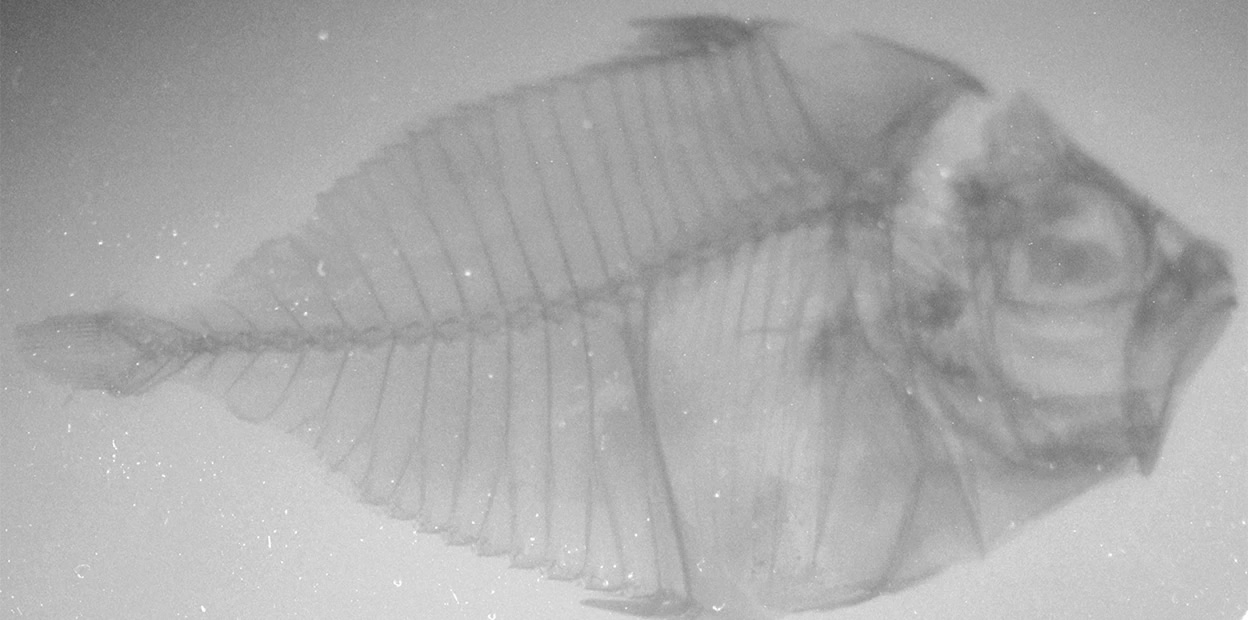
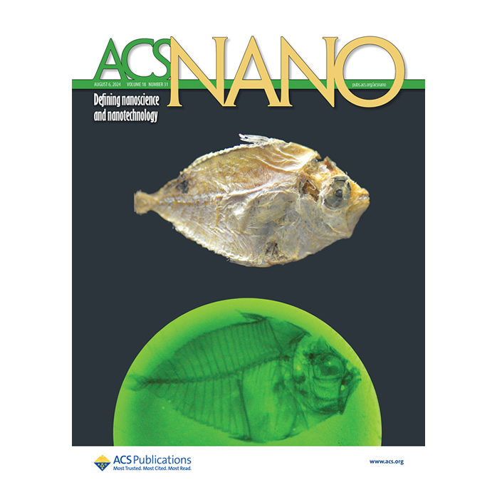
Nanomaterials for high-performance X-ray imaging. We report terbium-doped colloidal gadolinium oxysulfide nanoplatelets exhibiting near-unity photoluminescence quantum yields as promising X-ray scintillating nanomaterials. High resolution radioluminescence imaging of a small dried fish revealed the fish’s skeleton with exceptional detail.
[ACS Nano] [Front Cover]
[Front Cover, JPG]
[Publications]
Giant Negative Electrostriction in Polymer Nanofibers
Polymer biocompatible electromechanical sensors. We develop a scalable innovative nanofabrication methodology for the production of meters-long electrostrictive/piezoelectric nanofiber arrays for electromechanical (acoustic) sensors with unmatched sensing performance.
[Article]
[Publications]
Recent News
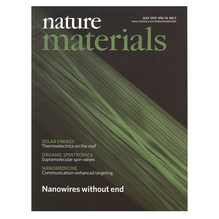
Journal Covers
Contributions to science & society
A New Top Down Nanofabrication Technique
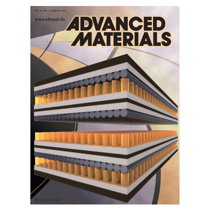
Transforming traditional fiber drawing into highly sophisticated nanomanufacturing toolbox. This work is the realization of a radically new nanofabrication scheme which allows mass-production of kilometer-long insulating, conducting, semiconducting, and piezoelectric nanostructures. Attaining ordered arrays of one-dimensional nanostructures in an extended flexible fiber with high yields will facilitate sought-after but up-to-now difficult applications such as the large area nanowire electronics and photonics, nanowire based scalable phase-change memory, nanowire photovoltaics, and emerging cell-nanowire interfacing.
Multimaterial Fiber-based Devices
Reinvention of fiber drawing in the age of nanotechnology. Dr. Mehmet Bayindir and his coworkers at MIT developed a radically new fabrication technique which allows production of kilometer long micro-structures having semiconducting, conducting and insulating constitutes at desired geometries. This transdisciplinary study constituted the fundamentals of a multimaterial fiber concept and are considered as a milestone in thermally drawn fiber technology due to their potential in advanced fiber devices and functional fabrics. The fabric would make curious clothing indeed, but it serves to demonstrate the level of sophistication reached in the design of optical fibers.
Biocompatible Electroactive Nanodevices
Piezoelectric/electrostrictive polymer nanosystems for smart skin, cardiac sensors, and energy harvesting. Typical piezoelectric materials used in device production do not inherently display piezoelectric properties, and must be processed through costly and complex fabrication steps prior to use. Dr. Bayindir and his team invented a new fabrication route for producing PVDF micro and nanostructures having record-high piezoelectric coefficient. Professor Mehmet Bayindir received an ERC Proof of Concept grant to support commercialization of piezo nanosystems for smart skin, cardiac sensors, and energy harvesting applications.
Large-area Nanowire Sensory Systems
Interfacing high-density nanosensors into microstructures. Integration of nanowires into functional devices with high yields and good reliability turned out to be a lot more challenging, and proved to be a critical issue obstructing the wide application of nanowire based devices and exploitation of their technical promises. Prof. Bayindir’s team demonstrated a relatively easy macro fabrication of a nanowire based imaging circuitry using a recently developed nanofabrication technique. This new approach makes it possible to devise extremely large nanowire devices on planar, flexible or curved substrates with diverse functionalities such as thermal sensors, phase change memory and artificial skin.
Triboelectric Nanogenerators
Next-generation self-powered energy harvesting devices. When nanostructured dielectric surfaces are in contact with each other or separated, there are positive and negative charges generated on coated electrodes depending on the triboelectric polarity of those dielectric materials. Kilometer-long nanostructures obtained by iterative size reduction technique developed by Bayindir group can be used to construct large-area energy harvesting systems by converting friction into useful energy source. Such compact, highly efficient nanogenerators can be used in wearable devices, self-powered sensory systems, and smart textiles.
Photonic Crystal Optoelectronic Digital Nose
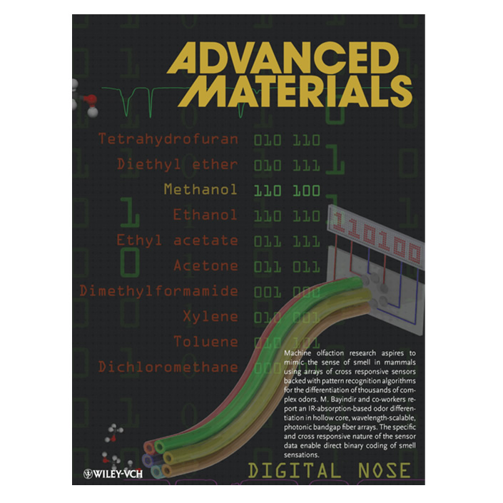
Digitizing smells. Professor Mehmet Bayindir’s team proposed a novel integrated functional fiber device with binary logic readout as contender of optoelectronic nose (digital photonic nose). The device uses photonic bandgap fibers for chemical sensing by means of infrared absorption spectroscopy. In the presence of such volatile molecules, transmission signal through the fibers selectively reduce depending on the the corresponding infrared absorption peaks of the analyte. Then, the total response of the fiber array is used to differentiate pre-determined chemicals with a novel binary logic tagging or other classical pattern recognition techniques. Their results can be considered as one of the first attempt for digitizing the smell.
A New Propagation Mechanism for Light
Propagation of photons through coupled-cavities in photonic crystals. Modulation of light in periodic structure has great potentials for obtaining all-optical logic operations. During his doctoral study, Dr. Bayindir proposed and demonstrated a new propagation mechanism for light through interacting cavities in photonic band gap materials. This important work was the first experimental realization of mode splitting and coupled-cavity waveguiding in photonic crystals. Dr. Bayindir’s work has attracted great attentions and cited over 500 times over the years. Dr. Bayindir won New Focus student awards for his achievements on the “couple-cavity waveguides”.
Institute of Material Science and Nanotechnology
Raising future nanoscientists. The graduate programs in Material Science and Nanotechnology (MSN) under the Institute of Material Science and Nanotechnology were established as “the first transdisciplinary graduate program in Turkey” with 4 students in 2007, since then the programs became very popular and attracted best students all around the world. As December 2015, the number of student reached a record high value, 110 from 13 nationalities. Professor Mehmet Bayindir was the deputy founding director of MSN between 2007 and 2013, and director of the programs between 2013-2016.
National Nanotechnology Research Center (UNAM)
Turkey’s top research institution according to Nature index. UNAM was established as a transdisciplinary state-of-the-art national research center with support of the State Planning of Organization of Turkey in 2006. UNAM’s mission is to shape the future by expanding the limits of science and technology, utilizing its resources and technical prowess as a national center to develop technologies that will play important roles in our daily lives, as well as to raise well-educated scientific personnel to ensure the continuity of Turkey’s technological and scientific development. Professor Mehmet Bayindir was the founding deputy director until 2013, and then the director of UNAM between 2013-2016.


